- 您现在的位置:买卖IC网 > Sheet目录1905 > ATMEGA48PA-MMNR (Atmel)MCU AVR 4KB FLASH 20MHZ 28QFN
141
8161D–AVR–10/09
ATmega48PA/88PA/168PA/328P
16. Timer/Counter0 and Timer/Counter1 Prescalers
113 share the same prescaler module, but the Timer/Counters can have different prescaler set-
tings. The description below applies to both Timer/Counter1 and Timer/Counter0.
16.1
Internal Clock Source
The Timer/Counter can be clocked directly by the system clock (by setting the CSn2:0 = 1). This
provides the fastest operation, with a maximum Timer/Counter clock frequency equal to system
clock frequency (f
CLK_I/O). Alternatively, one of four taps from the prescaler can be used as a
clock source. The prescaled clock has a frequency of either f
CLK_I/O/8, fCLK_I/O/64, fCLK_I/O/256, or
f
CLK_I/O/1024.
16.2
Prescaler Reset
The prescaler is free running, i.e., operates independently of the Clock Select logic of the
Timer/Counter, and it is shared by Timer/Counter1 and Timer/Counter0. Since the prescaler is
not affected by the Timer/Counter’s clock select, the state of the prescaler will have implications
for situations where a prescaled clock is used. One example of prescaling artifacts occurs when
the timer is enabled and clocked by the prescaler (6 > CSn2:0 > 1). The number of system clock
cycles from when the timer is enabled to the first count occurs can be from 1 to N+1 system
clock cycles, where N equals the prescaler divisor (8, 64, 256, or 1024).
It is possible to use the prescaler reset for synchronizing the Timer/Counter to program execu-
tion. However, care must be taken if the other Timer/Counter that shares the same prescaler
also uses prescaling. A prescaler reset will affect the prescaler period for all Timer/Counters it is
connected to.
16.3
External Clock Source
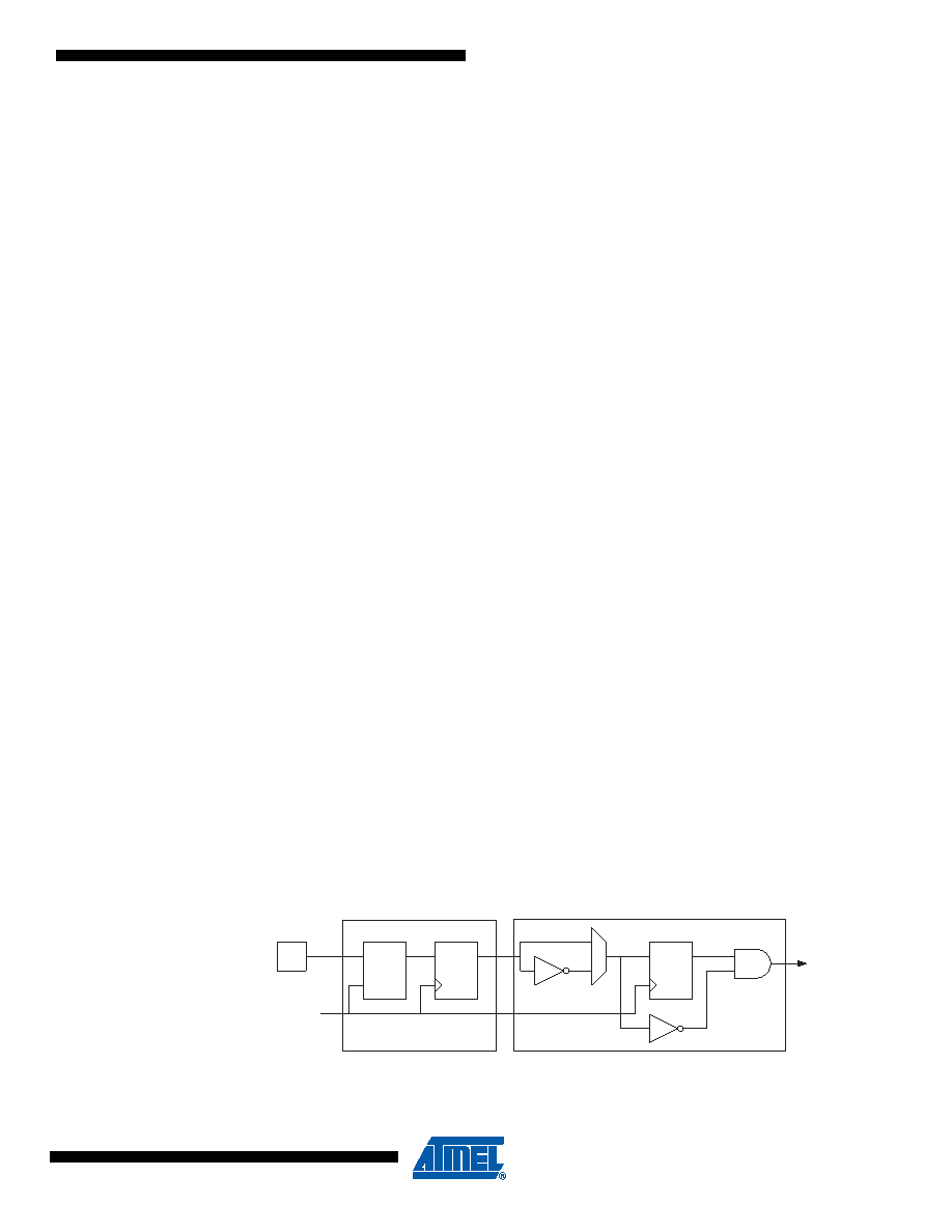
An external clock source applied to the T1/T0 pin can be used as Timer/Counter clock
(clk
T1/clkT0). The T1/T0 pin is sampled once every system clock cycle by the pin synchronization
logic. The synchronized (sampled) signal is then passed through the edge detector. Figure 16-1
shows a functional equivalent block diagram of the T1/T0 synchronization and edge detector
logic. The registers are clocked at the positive edge of the internal system clock (clk
I/O). The latch
is transparent in the high period of the internal system clock.
The edge detector generates one clk
T1/clkT0 pulse for each positive (CSn2:0 = 7) or negative
(CSn2:0 = 6) edge it detects.
Figure 16-1. T1/T0 Pin Sampling
The synchronization and edge detector logic introduces a delay of 2.5 to 3.5 system clock cycles
from an edge has been applied to the T1/T0 pin to the counter is updated.
Tn_sync
(To Clock
Select Logic)
Edge Detector
Synchronization
DQ
LE
DQ
Tn
clk
I/O
发布紧急采购,3分钟左右您将得到回复。
相关PDF资料
ATMEGA644P-B15MZ
IC MCU 8BIT 64KB FLASH 32VQFN
ATMEGA644V-10PU
IC AVR MCU FLASH 64K 40DIP
ATMEGA645V-8MI
IC AVR MCU FLASH 64K 1.8V 64QFN
ATMEGA649-16MI
IC AVR MCU FLASH 64K 5V 64QFN
ATMEGA649V-8MI
IC AVR MCU FLASH 64K 1.8V 64QFN
ATMEGA8515L-8JUR
MCU AVR 8KB FLASH 8MHZ 44PLCC
ATMEGA8515L-8PJ
IC MCU AVR 8K 5V 8MHZ 40-DIP
ATMEGA8535-16JUR
MCU AVR 8K FLASH 16MHZ 44PLCC
相关代理商/技术参数
ATMEGA48PA-MN
功能描述:8位微控制器 -MCU AVR 4KB FL 256B EE 512B SRAM 20MHz 105C RoHS:否 制造商:Silicon Labs 核心:8051 处理器系列:C8051F39x 数据总线宽度:8 bit 最大时钟频率:50 MHz 程序存储器大小:16 KB 数据 RAM 大小:1 KB 片上 ADC:Yes 工作电源电压:1.8 V to 3.6 V 工作温度范围:- 40 C to + 105 C 封装 / 箱体:QFN-20 安装风格:SMD/SMT
ATMEGA48PA-MNR
功能描述:8位微控制器 -MCU AVR 4KB FL 256B EE 512B SRAM 20MHz 105C RoHS:否 制造商:Silicon Labs 核心:8051 处理器系列:C8051F39x 数据总线宽度:8 bit 最大时钟频率:50 MHz 程序存储器大小:16 KB 数据 RAM 大小:1 KB 片上 ADC:Yes 工作电源电压:1.8 V to 3.6 V 工作温度范围:- 40 C to + 105 C 封装 / 箱体:QFN-20 安装风格:SMD/SMT
ATMEGA48PA-MU
功能描述:8位微控制器 -MCU AVR 4KB FLASH 20 MHZ,IND TEMP RoHS:否 制造商:Silicon Labs 核心:8051 处理器系列:C8051F39x 数据总线宽度:8 bit 最大时钟频率:50 MHz 程序存储器大小:16 KB 数据 RAM 大小:1 KB 片上 ADC:Yes 工作电源电压:1.8 V to 3.6 V 工作温度范围:- 40 C to + 105 C 封装 / 箱体:QFN-20 安装风格:SMD/SMT
ATMEGA48PA-MU@SL383
制造商:Atmel 功能描述:MCU 8-bit ATmega AVR RISC 4KB Flash 2.5V/3.3V/5V 32-Pin QFN EP T/R
ATMEGA48PA-MUR
功能描述:8位微控制器 -MCU AVR 4KB FLSH 256B EE 512B SRAM-20MHz IND RoHS:否 制造商:Silicon Labs 核心:8051 处理器系列:C8051F39x 数据总线宽度:8 bit 最大时钟频率:50 MHz 程序存储器大小:16 KB 数据 RAM 大小:1 KB 片上 ADC:Yes 工作电源电压:1.8 V to 3.6 V 工作温度范围:- 40 C to + 105 C 封装 / 箱体:QFN-20 安装风格:SMD/SMT
ATMEGA48PA-PN
功能描述:8位微控制器 -MCU AVR 4KB FL 256B EE 512B SRAM 20MHz 105C RoHS:否 制造商:Silicon Labs 核心:8051 处理器系列:C8051F39x 数据总线宽度:8 bit 最大时钟频率:50 MHz 程序存储器大小:16 KB 数据 RAM 大小:1 KB 片上 ADC:Yes 工作电源电压:1.8 V to 3.6 V 工作温度范围:- 40 C to + 105 C 封装 / 箱体:QFN-20 安装风格:SMD/SMT
ATMEGA48PA-PU
功能描述:8位微控制器 -MCU AVR 4KB FLASH 20 MHZ,IND TEMP RoHS:否 制造商:Silicon Labs 核心:8051 处理器系列:C8051F39x 数据总线宽度:8 bit 最大时钟频率:50 MHz 程序存储器大小:16 KB 数据 RAM 大小:1 KB 片上 ADC:Yes 工作电源电压:1.8 V to 3.6 V 工作温度范围:- 40 C to + 105 C 封装 / 箱体:QFN-20 安装风格:SMD/SMT
ATMEGA48PB-AN
功能描述:AVR AVR? ATmega Microcontroller IC 8-Bit 20MHz 4KB (2K x 16) FLASH 32-TQFP 制造商:atmel 系列:AVR? ATmega 包装:托盘 零件状态:有效 核心处理器:AVR 核心尺寸:8-位 速度:20MHz 连接性:I2C,SPI,UART/USART 外设:欠压检测/复位,POR,PWM,WDT I/O 数:27 程序存储容量:4KB(2K x 16) 程序存储器类型:闪存 EEPROM 容量:256 x 8 RAM 容量:512 x 8 电压 - 电源(Vcc/Vdd):1.8 V ~ 5.5 V 数据转换器:A/D 8x10b 振荡器类型:内部 工作温度:-40°C ~ 105°C(TA) 封装/外壳:32-TQFP 供应商器件封装:32-TQFP 标准包装:250